ABSTRACT: Atomistic understanding of the interaction between defects and active surface of the sensor is necessary for the developing devices detecting bio-and gas mixtures. We performed first principles computer simulations of the carbon dioxide (CO2) molecule adsorption on a ZnO surface in various configurations and location on the surface. It is shown that the tridentate configuration is the most energetically favorable, the binding energy of the molecule weakly depends on the surface coverage. The presence of intrinsic defects on the surface, such as an oxygen vacancy, leads to a small reduction of the binding energy. The observed data from the NEXAFS experiment and hypothetical formation of a new compound H2CO on the surface are discussed in the light of our calculations.
ABSTRACT: The ferroelectric distortions in perovskites were a subject of numerous investigations for a long time. However, some controversial results still exist, coming from the analysis of diffraction (X-ray, neutron or electron) data and X-ray absorption spectra. In this study, our goal was to revisit these classical materials using recently developed methods without imposing any predefined structural model. Local environment around A-type atom in ABO3 perovskites (SrTiO3, BaTiO3, EuTiO3) was studied by X-ray absorption spectroscopy (XAS) in a wide range of temperatures (20–400 K). Using reverse Monte Carlo method enhanced by evolutionary algorithm, the 3D structure was extracted from the extended X-ray absorption fine structure (EXAFS) and interpreted in terms of the radial distribution functions (RDFs). Our findings show that both diffraction and XAS data are consistent, but reflect the structure of the material from different points of view. In particular, when strong correlations in the motion of certain atoms are present, the information obtained by XAS might lead to a different from expected shape of the RDF. At the same time, the average positions of all atoms are in good agreement with those given by diffraction. This makes XAS an important technique for studying interatomic correlations and lattice dynamics.
Local structure of A-atom in ABO3 perovskites studies by RMC-EXAFS,
Rad. Phys. Chem. (2019), doi:10.1016/j.radphyschem.2018.11.026.
Download
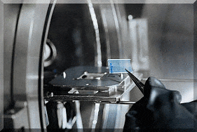
ABSTRACT: Reactive high power impulse magnetron sputtering (R-HiPIMS) has been demonstrated as a promising technique for the ZnO:Al (AZO) thin film deposition at low temperature with improved electrical properties compared to the reactive direct current magnetron sputtering (R-dcMS). However, there are not enough studies about the HiPIMS process using Zn/Al target itself. Additionally, AZO films have not been deposited with the pulse duration times long enough to allow the discharge to develop into the self-sputtering mode. C-V-t characteristics and the time average plasma optical emission spectra were studied as a function of different sputtering parameters, such as frequency, average power, pulse duration time, and oxygen flow rate. AZO films were deposited on glass substrates without intentional heating by R-HiPIMS using 500 μs long pulses. Structural, electrical and optical properties of the AZO films were studied as a function of peak current. Obtained peak power densities are relatively low compared to other metals due to the strong argon gas rarefaction, however, it is possible to increase the peak power density above 0.5 kW/cm2 by increasing the time between pulses or the average power to reach the HiPIMS regime. If the pulse duration time is 500 μs, the sustained self-sputtering discharge can be observed when the peak power density is above 0.3 kW/cm2. The peak current is sensitive to the oxygen content in the sputtering atmosphere so that it can be used as a control parameter for the reactive sputtering. The lowest obtained resistivity of the AZO films is 1.0 × 10⁻³ Ωcm with the transmittance around 70% in the visible light range. From the XRD measurements, there is the indication of existing zincblende structural phase in the R-HiPIMS deposited AZO films using high oxygen partial pressur.
ABSTRACT: In this work, a simple catalyst-free vapour-solid deposition method is applied for controlled obtaining of two types (planar and disordered) continuous Bi2Se3 nanostructured thin films on different (fused quartz/glass, mica, graphene) substrates. Performed for the deposited thin films transport and thermoelectric characterization (type, concentration and mobility of the main charge carriers, Seebeck coefficient and power factor) showed that proposed deposition method allows to fabricate “low-doped” Bi2Se3 thin films with power factor comparable and even higher than reported for the Bi2Se3 thin films fabricated by molecular beam epitaxy technique.
ABSTRACT: In this work, a simple catalyst-free vapour-solid deposition method was applied for controlled deposition of two types (planar and disordered) of continuous Bi2Se3 nanostructured thin films on different (fused quartz/glass, mica, graphene) substrates. Characterisation of electron transport (type, concentration and mobility of the main charge carriers) and thermoelectric properties (Seebeck coefficient and power factor) showed that proposed in this work deposition method allows to obtain Bi2Se3 thin films with power factor comparable and even higher than reported for the Bi2Se3 thin films grown by molecular beam epitaxy technique. Power factor of the best obtained thin films can be significantly improved by introduction Sb or Fe dopants in low concentrations.
ABSTRACT: In this study, pentagonal Ag and Au nanowires (NWs) were bent in cantilever beam configuration inside a scanning electron microscope. We demonstrated unusual abrupt elastic-to-plastic transition, observed as sudden change of the NW profile from smooth arc-shaped to angled knee-like during the bending in the narrow range of bending angles. In contrast to behavior of NW in tensile and three-point bending test, where extensive elastic deformation was followed by brittle fracture, in our case after the abrupt plastic event NW was still far from fracture and enabled further bending without breaking. Moreover, we found that if NWs are coated with alumina, abrupt plastic event is not observed and NWs can withstand severe deformation in elastic regime without fracture. Mechanical durability under high and inhomogeneous strain fields is an important aspect of exploiting of Ag and Au NWs in applications like waveguiding or conductive network in flexible polymer composite materials.
ABSTRACT: In the present paper we investigate the effect of heat-treatment on geometry and mobility of
Au nanoparticles (NPs) on Si substrate. Chemically synthesized Au nanoparticles with
median diameter of 14 nm were annealed at 200°C, 400°C, 600°C and 800°C for 1 hour.
Geometry changes from faceted towards more rounded shapes were observed already for
200oC and increased further for higher temperatures. According to Kinetic Monte Carlo
simulations NPs become rounded through the minimization of the surface area and
transitioning to lower energy surface types {111} and {100}. Next, NPs were manipulated
with atomic force microscope and it was found that the higher is annealing temperature, the
less energy was required to displace the particle. However, after treatment at 800°C particles
became immovable. We attributed this surprising effect to diffusion of gold into Si and to the
growth of SiO2.
ABSTRACT: Mechanical characterisation of individual nanostructures is a challenging task and can greatly benefit from the utilisation of several alternative approaches to increase the reliability of results. In the present work, we have measured and compared the elastic modulus of five-fold twinned gold nanowires (NWs) with atomic force microscopy (AFM) indentation in three different test configurations: three-point bending with fixed ends, three-point bending with free ends and cantilevered-beam bending. The free-ends condition was realized by introducing a novel approach where the NW is placed diagonally inside an inverted pyramid chemically etched in a silicon wafer. In addition, all three configurations were simulated with a finite element method to obtain better insight into stress distribution inside NWs during bending depending on test conditions. The free-ends configuration yielded elastic modulus similar to a classical fixed-ends approach (88 ± 20 GPa vs 87 ± 16 GPa), indicating the reliability of the proposed method. At the same time, the free-ends configuration benefits from a more favourable NW position relative to the probe with facet facing upwards in contrast to the sharp edge in the case of fixed ends. From the other hand, the free-ends configuration was less suitable for strength measurements, as NW can run into the bottom of the inverted pyramid because of a higher degree of deformation before fracture. The cantilevered-beam configuration was less suitable for mechanical testing with indentation because of the instabilities of the free end under the AFM probe.
 Login
Login Ongoing projects