|
|
| Thin Films Laboratory website » Equipment |
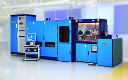
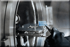
Multifunctional cluster tool - SAF25/50
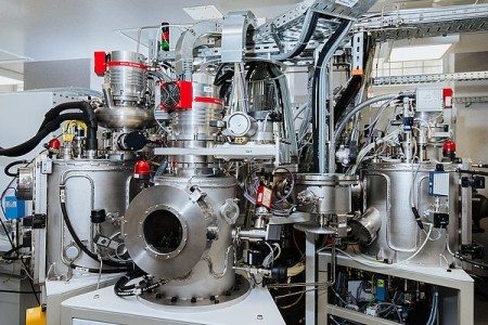 Category Category
Materials synthesis and treatment; Cleanrooms
Manufacturer and Model
Sidrabe - SAF25/50
Specifications
- Substrate: glass, metal, plastic, ceramic
- Substrate size: 25 x 25 or 50 x 50 mm
- Substrate temperature: - 40 … + 400ºC (depends on the process)
- Base pressure: 1·10-7 Torr
- Installed power: 50 kW
Applications and capabilities
The SAF25/50 multifunctional R&D cluster tool is intended for research and development works as well as for feasibility studies and more general academic work in the field of thin film technologies.
The tool is a multifunctional, expandable, modular and flexible system. The tool comprises an input/output chamber with ion gun, central substrate transfer chamber with radial telescopic transport arm and up to 7 deposition chambers. Substrate is positioned horizontally on a holder. Deposition zones are configured for substrate rotation or displacement during upward deposition.
 Tool multifunctionality and flexibility is founded on the following key features: Tool multifunctionality and flexibility is founded on the following key features:
- Each chamber can operate independently due to individual pumping means, controls and utility connections.
- Deposition chambers and deposition sources are interchangeable.
- The central transfer chamber prevents process cross-contamination and ensures substrate transfer without venting of the chambers.
- Various types of deposition sources including sublimation thermal cells, resistive boats, crucibles and sputter magnetrons can be integrated.
- Twin, single and dual sputter magnetrons can be powered by DC, pulsed DC, MF and RF power supplies.
- Contact and contactless cooling and heating of the substrate is offered.
- Glove box for substrate loading in inert gas atmosphere and substrate magazine can be added.
- Preliminary agreed number of blanked-off flanges installed on the chambers allows attaching customized instrumentation and technological accessories.
- Basic configuration of the pumping system includes turbomolecular and two-stage dry mechanical pumps.
- The control system can operate in a semi-automatic and manual mode.
Responsible persons: Mārtiņš Zubkins, Lauris Dimitročenko
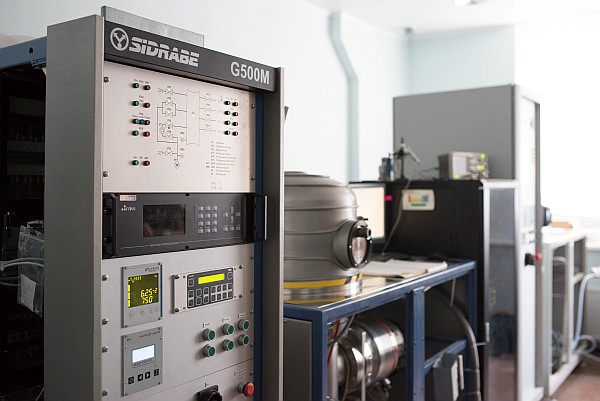
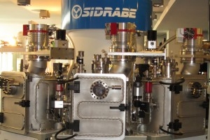
Magnetron sputtering unit - G500M
Key features:
- Chamber volume: 0,1 m3;
- The pumping system consists of turbomolecular and mechanical pumps with and an adjustable gate valve;
- Ar, O2, N2, Ar+H2, H2 flows controlled by MKS mass flow controllers;
- 2 rectangular 150 x 75 mm (or 200 mm x 100 mm) magnetrons in each chamber;
- Substrate temperature between 800 OC and liquid nitrogen (- 196 oC);
- Sputtering modes: DC, pulsed-DC, HIPIMS with unipolar pulses, MF and HIPIMS with bipolar symmetric and asymmetric pulses;
- OES and voltage process control for reactive processes;
- Substrate linear movement.
Responsible person: Mārtiņš Zubkins
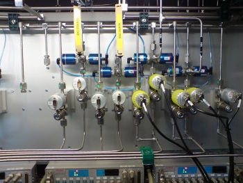
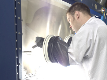
Metal-organic chemical vapour deposition (MOCVD) unit - AIX200 RF
 MOCVD reactor (Aixtron AIX-200RF) is available for the synthesis of thin films involving metals, liquid metal-organic compounds and gaseous non–metal chemical hydride and oxide gases. The Control of the rate of reactants flow is provided using thermostats for liquid metal-organic compounds, and carrier gas (N 2, H 2) flow. The control of non-metal chemical hydride gases flows involves both the carrier gas and precursor flow. The Present MOCVD equipment has the following chemical reactants installed: SiH 2 (6N), SiH 2 200ppm H 2 mixture, NH 2 – nitrogen source (6N), N 2, H 2 carrier gases (purity 2ppb), metal-organic lines: metal sources (Ga, Al, Zn, Mg, In) – TMGa, 2 x TMIn, TEGa, 2 x TMAl, CpMg, DEZn, oxygen sources – NO, N 2O. The equipment will be renovated for the synthesis of classic LED structures, as well as for the synthesis of Si, ZnO, and group III nitride 1D nanostructures. There is a possibility to dope the materials, in order to obtain n- or p-conductivity. MOCVD equipment is used to manipulate chemical reactants creating different 1D, 2D, and hybrid structures. The reactor has been designed for III-V nitride semiconductor layer deposition, has been used for GaN blue light LED structure deposition.
The system comprises:
- precursor transport system;
- cols wall reactor with RF induction heatable susceptor for temperatures up to 1200oC;
-
vacuum system;
- exhaust gas filters;
- control panel;
- glove-box for sample input.
Responsible person: Lauris Dimitročenko
Atomic layer deposition (ALD)
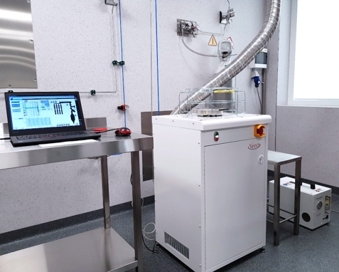 Atomic layer deposition (ALD) is a subclass of chemical vapour deposition that is based on the sequential use of a gas phase chemical process. The majority of ALD reactions use two precursors, reacting with the surface of a material one at a time in a sequential, self-limiting, manner. Through the repeated exposure to separate precursors, a thin film is deposited. The system can be used for fabrication of semiconductor devices, and for synthesis of nanomaterials.
Key components and features:
- Substrate temperature: up to 400 °C;
- Materials available: Al2O3, HfO2, ZnO, AZO, TiO2, AlN;
- Exposure ModeTM deposits films with ultra high aspect ratio (>2000:1);
- Stacks of two materials;
- Substrate size: up to 100 mm diameter x 6.4 mm thickness;
- Ozone generator and Low vapor pressure delivery.
Model: Veeco ALD Savannah S100
Responsible persons: Boris Polyakov, Edgars Butanovs
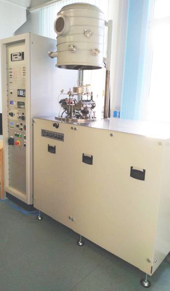
Pulsed Laser Deposition (PLD)
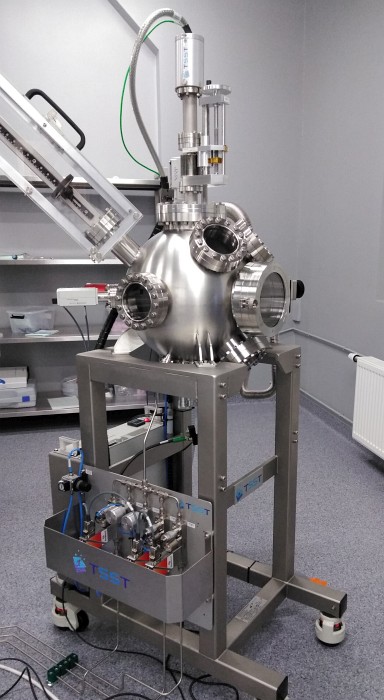 Pulsed Laser Deposition (PLD) will be developed for production of thin films and heterostructures from various materials with complicated stoichiometry. PLD will allow a one-to-one transfer of elements from target to substrate, which is a strong advantage for the deposition of multiple element systems. Different atmospheres of deposition allow for varying of film properties in a wide range. We plan to deposit high-quality oxide and sulfide thin films, including perovskites, gallium oxide based materials and layered 2D transition metal dichalcogenides.
The system comprises:
- pulsed excimer laser;
- laser optics;
- two vacuum chambers:
- for oxide layer deposition: base pressure 10
-7 mbar, Ar, O2, N2 gases, rotatable target system with 4 targets;
- for anticorrosion sulfide and other oxygen free layer deposition: H2S, Ar, N2 gases, rotatable target system with 5 targets;
- heatable substrate holder for temperatures up to 900oC;
- vacuum system.
Manufacturer: Twente Solid State Technology (TSST)
Responsible person: Edgars Butanovs
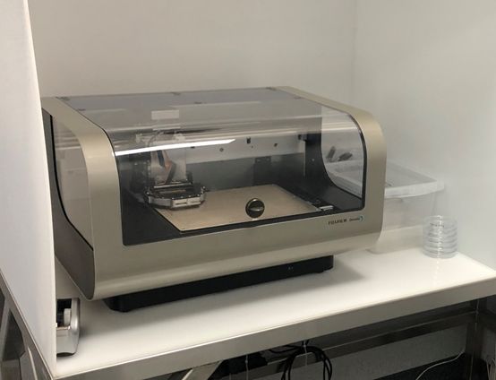
Ink-Jet Dimatix Materials Printer
The Dimatix Materials Printer (DMP) is a laboratory and limited production tool that enables researchers, scientists, and engineers to evaluate the use of ink jetting technology for new manufacturing and analytical processes. It is designed to be convenient and easy to use to carry out “proof of concept” and development work using ink jet technology. It does have extensive capabilities to allow increased experimental sophistication to optimize process parameters for the user’s applications as the user gains familiarity with the system.
Responsible person: Boris Polyakov
Hall Effect Measurement System (Van der Pauw configuration) - HMS-5000
 Category Category
Materials characterization
Manufacturer and Model
Ecopia - HMS-5000
Specifications
- Sample size: 5 mm x 5mm up to 15mm x 15mm
- Resistivity: 10-4 to 107 (Ohms-cm)
- Magnet: Permanent magnet, 30 mm diameter
- Magnet Flux Density: 0.55 T nominal ±1% of marked value
- Mobility (cm2/Volt-sec): 1 ~ 107
- Concentration (cm-3): 107~ 1021
- Current Source: Range: 1 nA - 20 mA, Compliance: 12 VMinimum Hall Voltage: 1 μV
- temperature Ranges: 80K to 350K
Applications and capabilities
Characterization of various materials including all semiconductors including Si, SiGe, SiC, GaAs, InGaAs, InP, GaN (N Type & P Type can be measured), metal layers, oxides, etc.
Testing of Temperature vs carrier density, mobility,resistivity, hall coefficient, conductivity, etc.
Responsible person: Mārtiņš Zubkins
|
|
|
 Login
Login Ongoing projects