To enhance the institute (ISSP) focus on thin films science and technology the Thin Films Laboratory has been established in 2017.
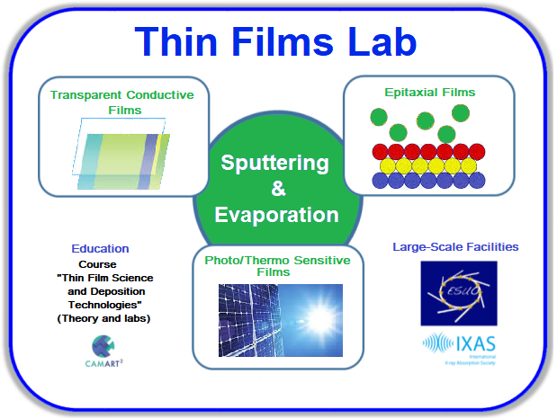
The methods of film deposition include evaporation (thermal and pulsed laser deposition) and magnetron sputtering (DC, RF, HIPIMS) technologies.
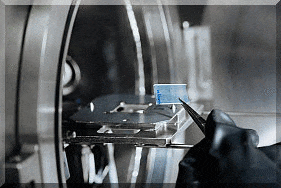
The Laboratory is well on equipped instrument park of technological facilities.
The Thin Films Laboratory mainly focused on thin film deposition and nanocoating of a wide variety of inorganic materials, using different deposition techniques from existing and new tools, including:
- PVD vacuum multifunctional R&D cluster SAF25/50 (thermal, e-beam and magnetron sputtering),
- magnetron sputtering G500M cluster including High Power Impulse Magnetron Sputtering (HiPIMS),
- PLD (Pulsed Laser Deposition),
- MOCVD (Metal Organic Chemical Vapour Deposition), and
- ALD (Atomic Layer Deposition).
The deposition tools are operated by
highly skilled staff, enabling the deposition of novel materials as required by internal projects and external customers.
Current scientific projects are targeted on the development of novel advanced materials and coatings. The laboratory takes part and submitt applications for projects of H2020, ERAF, LZP, EUROfusion and others.
In recent years we have developed nanocoating technologies approved by patents and papers.
The laboratory have patented and published technologies of deposition:
- an antiviral, yeasticidal and antibacterial nanocoatings;
- novel R-HiPIMS technology of deposition of functional TMO (transition metal oxides) thin films and multilayers on flexible substrate and upscale the process
- cryogenic process - p-type ZnO-ZnO2;
- HIPIMS dual magnetron yttrium monoxide;
- novel thin films ReO3-WO3 and ReS2 with advanced electric and optical properties and others.
The Thin Films Laboratory is granted by many high rating scientific proposals for 2021-2024 years.
The Thin Films Laboratory is well positioned to explore new materials for different applications and is further supported by an extensive publication track-record in both basic and applied physics journals.
Deposition technologies developed in the last years are widely and extensively used for thin films and coatings productions.
Especially HIPIMS processes using dual magnetron sputtering play an important role for deposition new materials: ZnO-IrO2, ZnO-Al, ReO3-WO3, NiO-IrO2, WO3/Cu/WO3.
As evaluated by EU referees, the proposals are of excellent quality with the goal to develop novel and advanced procedures for metal oxide sputter coating of extended surfaces. Such coatings are extremely versatile and used in a variety of electrooptical and semiconductor based applications.
The laboratory collaborates with the largest vacuum technology industry among the Baltic countries: SIDRABE VACUUM, Ltd., SCHAEFFLER BALTIC, Ltd., GROGLASS, Ltd., ALFA, Inc..
Cutting-edge plasma HIPIMS and dual magnetron co-sputtering technologies developed are approved by many EU patents and become the process of choice in many EU and LV applied projects and applications:
- antiviral and antibacterial,
- transparent conducting oxides (TCO),
- multifunctional electrochromic and photochromic thin films etc.
The existing equipment, together with the accumulated experience, provides an opportunity for extensive scientific research, discovery and development.
The Laboratory provides thin film deposition services of a wide variety of materials, using different techniques from existing and new deposition tools, including the multifunctional R&D cluster plant and MOCVD.
The SAF25/50 multifunctional R&D cluster plant installed at ISSP UL cleanrooms in 2015 and upgraded in 2019 is intended for research and development in the field of thin film technologies. The plant is a multifunctional, expandable, modular and flexible system. The plant comprises an input/output chamber with ion gun, a central substrate transfer chamber with radial telescopic transport arm and up to 7 deposition chambers. The substrate is positioned horizontally on a holder. Deposition zones are configured for substrate rotation or displacement during upward deposition.
Pulsed laser deposition (PLD) is a valuable tool for production of thin films and epitaxial heterostructures from various materials with complicated stoichiometry. PLD allows a one-to-one transfer of elements from target to substrate, what is a strong advantage for the deposition of multiple element systems. Different atmospheres (Ar, O2, N2, H2, H2S) of deposition allow varying of properties of films in a wide range: ZnO, Ga2O3, MoS2, etc. ISSP UL has experience in making high-quality thin films of perovskite structures by PLD as lead-free ferroelectric thin films for non-volatile memories and NEMS, in studying structure and surface topology (by AFM), in characterization of dielectric and electromechanical properties.
MOCVD reactor Aixtron (AIX-200RF) is available for the synthesis of epitaxial thin films using liquid metal-organic compounds and gaseous non–metal chemical hydride and oxide gases. The equipment is suitable for the synthesis of classic LED structures, Si, ZnO, and group III nitride 1D nanostructures, as well as for deposition of functional ultra-wide bandgap gallium oxide and metal oxide (GaMeO) thin films and multilayers for optoelectronic and electronic applications. Novel reflecting optical coatings (on mirrored sapphire substrate - MSS) for LED device structure fabrication based on MOCVD grown epitaxial Ga2O3/Al2O3 multilayers (prototype, patents, technology description) for adaptive optics. There is a possibility to dope the materials, in order to obtain n- or p-conductivity. MOCVD equipment provides wide possibilities to manipulate chemical reactants creating different 1D, 2D, and hybrid structures.
Atomic layer deposition (ALD) is a subclass of chemical vapour deposition based on the sequential use of a gas phase chemical process. The system can be used for fabrication of semiconductor devices, and for synthesis of nanomaterials.
Thanks to Thin Films Laboratory nowadays ISSP UL becomes a recognised centre of excellence for thin film nanotechnologies in Baltic countries.
Laboratory is also involved in the teaching process at the University of Latvia and provides students with opportunities to participate in research activities during Bachelor, Master and Doctoral level programs.
 Login
Login Ongoing projects