The aim of the Smart Windows for Zero Energy Buildings (SWEB) project is to develop world-leading research on functional materials and their SWEB applications, to advance teaching capacity and to foster institutional governance changes towards excellence and sustainability. Institute of Solid State Physics (ISSP) of the University of Latvia is the leader of Functional Materials and Coating research in Latvia. It concentrates significant resources in materials research, testing, advanced training, and innovation. ISSP key technologies are based on inorganic and organic thin film deposition on a wide variety of materials, using different advanced deposition techniques from existing and new tools. The deposition tools are operated by highly skilled staff, enabling the deposition of novel materials as required by internal research projects and external customers. Currently several ongoing research projects aim at the development of novel advanced materials and coatings for SWEB.
ERA Chair SWEB will establish high-quality researcher and expert team by synergistically merging chromogenic SW materials and complementary competencies at ISSP and bridging the gap between research and technology transfer. The knowledge gained will increase research excellence, visibility, and attractiveness of ISSP and Latvia in general, thus enhancing participation in ERA. Furthermore, these ambitious research and innovation goals targeting emerging next-generation chromogenic SW development will lay the foundation for further technical development and innovative production of SWEB in other regions of the EU. Ultimately, society as a whole will benefit from excellent job opportunities for specialists, more youths are drawn to prestigious technology and engineering-oriented higher education, a bridge between R&D and the public, and consumers will indirectly benefit from shorter prototype to market development cycles of targeted chromogenic SW.
ISSP UL main objectives:
1. Human capital development benefits. With support of the ERA Chair and team, the SWEB project will increase the R&D&I capacity of ISSP by developing its research potential in the areas of materials science, positively contributing to the activities of the existing Centre of Excellence (CAMART2).
2. Development of new energy saving and chromogenic materials and devices, developing scalable deposition methods, stability testing protocols for photochromic and thermochromic films, indoor and outdoor testing.
3. Publication and knowledge transfer benefits. The publication of the obtained scientific results in high- impact peer-review journals will contribute to higher recognisability of ISSP and the possibility to gain more external funding.
4. Long-term benefits in sustainable energy and economy by the SWEB project contribution to the Solutions for meeting crucial challenges in the development of a resource-efficient society; and by establishment of the Briefing Demo Centre and EU joint graduate school on SW and zero energy buildings as a long-term impact after the finalisation of the SWEB, based on the strong R&D&I and stockholder network developed during the project.
5. Innovation transfer to start-ups and spin-off businesses. The project results will provide a strong background for further development of technology within commercialization activities at ISSP.
Total funding: 4 157 054.50 Eur, 100% financed by European Commission
Duration: 01.10.2022. – 30.09.2025.
Identification number: 101070310
Project aim:
The aim of Sestosenso is a new embedded proximity and tactile sensing technology development for a robot body, providing unified proxy-tactile perception of an environment required to control the robot's actions and interactions safely and autonomously. The advancement of this sensing technology for collaborative robotics applications starts from the hardware and evolves up to the cognitive perception and control levels through specific electronics and software development.
Project summary:
Sestosenso develops technologies for the next generations of collaborative robots capable of self-adapting to different time-varying operational conditions and capable of safe and smooth adaptation from autonomous to interactive when human intervention is required either for collaboration or training/teaching. The project proposes a new sensing technology from the hardware and up to the cognitive perception and control levels, based on proximity and tactile sensors embedded in the robot body, providing unified proxy-tactile perception of an environment required to control the robot's actions and interactions safely and autonomously. Sestosenso is motivated by the industrial need to integrate workers with robots and the need for robots that could operate safely without out-of-the-robot infrastructure, thus reducing robot setup times and costs and increasing the flexibility of the shopfloor configuration. The Sestosenso technology is demonstrated by three Use Cases of industrial interest: cooperative assembly (automotive), handling and packaging (logistics), and cooperative harvesting (agriculture).
Expected scientific results:
Hybrid sensor integration using printed electronic on conformable substrates
Manufacturing of tactile sensors onto conformable substrates
Optical tactile sensing
Proximity technology for robot sensing
Proxy-tactile data driven processing for control and human robot interaction
Proxy-tactile human robot interaction and whole-body handling of objects
Tasks at ISSP, UL:
ISSP UL contributes to materials evaluation and multimodal transduction solutions selection, manufacturing processes evaluation and selection, sensor layout and electronic design and assessment of integrated sensor physical performance.
Furthermore, ISSP UL leads four tasks in Sestosenso project:
Reference framework monitoring
Modelling and evaluation of innovative optical tactile transducers
Technical and Scientific Management
Operational and Quality Procedures
ISSP UL is responsible for 2 deliverables and 1 milestone related to optical tactile sensor development.
Project aim: is to develop advanced deposition technology of metal hydride and borohydride films, and study the influence of growth process parameters on the thin film structure and properties.
Project summary:
Reactive High Power Impulse Magnetron Sputtering (r-HiPIMS) deposition technology has a huge potential for manufacturing coatings with properties exceeding those of state of the art. The available research activities have mainly been the HiPIMS deposition of metals (Ar plasma), metal oxides by reactive process (Ar+O2), and metal nitrides (Ar+N2), but deposition of metal hydrides (Ar+H2) has not yet been demonstrated. Metal hydrides (MHx) and boro-hydrides M(BH4)x are a fascinating and important class of materials that can be used for storage and other energy applications, as far as Hydrogen storage will be a key technology for energy utilization in the 21st century. Also, lanthanide hydrides (LnHx) are unique classes of materials with a rich spectrum of physical properties. The project proposes to produce MHx and M(BH4)x (M: alkali-earth Mg, transition metals Ti and Y, lanthanides La and Eu) in the thin film form by r-HiPIMS and do in-depth characterisation by advanced in-lab techniques – XRD, XPS, SEM, TEM, Raman and UV-Vis-NIR spectroscopy, and spectroscopic ellipsometry. The project aims to study the relationship between the HiPIMS deposition parameters (impulse durations, sputtering power, pressure, substrate temperature) and chemical composition, properties, structure and density. HiPIMS sputtering has been chosen as the deposition technique since it is widely used in both lab-scale and industry with possible up-scaling.
PROJECT PROGRESS INFORMATION
Period:
01.04.2023 – 31.03.2026 | March 31, 2023
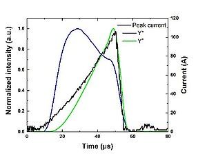
During the specified time frame, a vacuum physical vapour deposition system was successfully prepared to realize reactive high power impulse magnetron sputtering (r-HiPIMS). The system is equipped with balanced magnetrons and the necessary process gases – Ar and H2. We conducted preliminary experiments on an yttrium (Y) target by sputtering the target in both inert (Ar) and reactive (Ar+H2) atmospheres. Our system is equipped with a HiPIMS power source, alongside a high time-resolved spectrometer to detect changes in plasma emission line intensities during a pulse. Figure 1 shows an example of the change in emission intensities of excited Y atoms (Y*) and ions (Y+) during a 50 µs sputtering pulse. Both the discharge current peak value of 105 A and the intense Y+ emissions correspond to the HiPIMS mode. Emission line intensity directly depends on the concentration of relevant particles in the plasma and provides essential information for further process optimization. We successfully deposited the first thin films of yttrium hydride (YH2) and yttrium oxyhydride (YHO) on glass substrates using the r-HiPIMS process.
Figure 1. Evolution of discharge current and the intensity of excited Y atom and ion emission lines (410.2 nm and 437.5 nm, respectively) during a 50 µs-long HiPIMS pulse.
Total funding: 300 000 EUR
Project duration: 2023 - 2025
Identification number: lzp-2022/1-0311
Project aim:
The objective of this research project is to experimentally and theoretically investigate the effect of strain in MgB2 nanocoatings on its superconductivity transition temperature using various approaches of strain engineering in a core-shell nanowire configuration.
Project summary:
Superconducting nanowire single-photon detectors (SNSPDs) are considered as the primary emerging technology for single-photon detection in next-generation quantum telecommunications and cryptography, environment analyses, laser rangefinders, low-noise scientific measurements etc., however, their widespread use is still limited mainly due to the very low operating temperatures, which requires complex and costly cryogenics. Magnesium diboride MgB2 is a binary compound with one of the highest superconducting transition temperatures at 39 K, which could be raised even higher by creating anisotropic strain in the crystal lattice. In this fundamental research project, we plan to investigate the effect of strain in MgB2 nanocoatings on its superconductivity transition temperature using various novel approaches of strain engineering in a core-shell nanowire (NW) configuration. The experimental work will be supported by ab initio density functional theory and finite element calculations. The main scientific results will include: experimental elucidation of the effect of strain in MgB2 nanocoatings on its superconductivity transition temperature, new technological knowledge on the magnetron sputtering synthesis of MgB2-based thin films and nanostructures, and development of combinative state-of-the-art nanomechanical tests of individual NWs. The project is realized in cooperation with the Latvian Quantum Initiative (quantumlatvia.lu.lv).
Total budget: 299 991 EUR
Duration (years): 2021 - 2023
Agreement No: LZP-2020/1-0026
In this project, we plan to develop and to investigate new charge density wave (CDW) material hybrid nanowire heterostructures suitable for photodetection in a wide wavelength range. The project idea is based on the combination of CDW material shell and semiconductor nanowire core, resulting in hybrid core-shell nanowires. We plan to investigate layered CDW hybrid systems growth on substrates with a hexagonal crystal structure that are stable in a corrosive sulfur atmosphere, such as GaN, InN, and ZnS, and on materials that can be converted to sulfides, such as ZnO (ZnS). The layered CDW materials to be studied are mainly transition metal chalcogenides (TaS2, VS2, VSe2, TiSe2, etc.). Several synthesis methods will be used and compared to grow the shell of the CDW material (eg pulsating layer deposition, magnetron sputtering, etc.). The electronic and optoelectronic properties of the core-shell nanowires will be studied by integrating them into a single nanowire device, such as a field effect transistor and a phototransistor. The project includes theoretical calculations aimed at studying the structure and properties of the core-shell interface.
ABSTRACT: One-dimensional (1D) nanostructures – nanowires (NWs) – exhibit attractive properties for integration in different types of functional devices. Their properties can be enhanced even further or tuned for a specific application by combining different promising materials, such as layered van der Waals materials and conventional semiconductors, into 1D-1D core–shell heterostructures. In this work, we demonstrated growth of GaN-MoS2 and GaN-WS2 core–shell NWs via two different methods: (1) two-step process of sputter-deposition of a sacrificial transition metal oxide coating on GaN NWs followed by sulfurization; (2) pulsed laser deposition of few-layer MoS2 or WS2 on GaN NWs from the respective material targets. As-prepared nanostructures were characterized via scanning and transmission electron microscopies, X-ray diffraction, micro-Raman spectroscopy and X-ray photoelectron spectroscopy. High crystalline quality core–shell NW heterostructures with few-layer MoS2 and WS2 shells can be prepared via both routes. The experimental results were supported by theoretical electronic structure calculations, which demonstrated the potential of the synthesised core–shell NW heterostructures as photocatalysts for efficient hydrogen production from water.
ABSTRACT: During the synthesis of heterostructured nanomaterials, unwanted structural and morphological changes in nanostructures may occur, especially when multiple sequential growth steps are involved. In this study, we describe a synthesis strategy of heterostructured ZnS/Al2O3/MoS2 core-shell nanowires (NWs), and explore the role of the Al2O3 interlayer during synthesis. Core-shell NWs were produced via a four-step route: (1) synthesis of ZnO NWs on a silicon wafer, (2) deposition of thin Al2O3 layer by ALD, (3) magnetron deposition of MoO3 layer, and (4) annealing of the sample in the sulphur atmosphere. During sulphurization, ZnO is converted into ZnS, and MoO3 into MoS2 , while the Al2O3 interlayer preserves the smooth surface of an NW required for the growth of a continuous MoS2 shell. The resulting ZnS/Al2O3/MoS2 core-shell NWs were characterized by transmission electron microscopy, X-ray diffraction and photoelectron spectroscopy, Raman spectroscopy, and optical photoluminescence spectroscopy. A reported strategy can be used for the synthesis of other core-shell NWs with a transition metal dichalcogenides (TMDs) shell to protect the NW core material that may otherwise be altered or damaged by the reactive chalcogenides at high temperatures.
Motivated by the high demand for transparent electrical conductors, in this fundamental project we will investigate the topological-like electrical conductivity in Ga2O3 thin films grown via MOCVD on different orientation (including off-axis) sapphire substrates that could be applied in Ga2O3 -based transparent electrodes in ultraviolet optoelectronic devices. The key result will be deeper physical understanding of sapphire substrate crystallographic orientation impact on topological-like metallic conductivity in β– Ga2O3 thin films. Information about epitaxial relations between the film and the substrate together with advanced in-depth film characterization methods might elucidate the surface conductivity mechanism. The origin of a such exceptionally robust conduction merits to be investigated more deeply, because it challenges our current understanding and ways to achieve solar-transparent conducting electrodes in a wide bandgap insulator.
The planned activities include establishment of the MOCVD process for growing epitaxial monocrystalline β–Ga2O3 thin films, investigation of as-grown thin film electrical properties together with detailed structural, compositional and optical characterization of the films by traditional laboratory and advanced synchrotron radiation methods with focus on surface properties and possible donor doping, and large-scale theoretical calculations to elucidate the possible surface conductivity mechanisms.
European Regional Development Fund projects
Total funding: The total budget is 500 000 EUR with ERAF contribution of 425 000 EUR.
Duration: 01.01.2022 - 30.11.2023
Identification number: Nr.1.1.1.1/21/A/050
Project aim:
The aim of this industrial research project is to develop advanced roll-to-roll (hereinafter R2R) physical vapour deposition (PVD) technology for large scale production of a new type of multifunctional antibacterial and antiviral (MABAV) coatings. We propose to produce and investigate MABAV materials in the form of thin films and multilayers with photochromic and transparent conducting multifunctionalities based on rare-earth oxy-hydrides (REHO) and metal oxides (MO) in combination with the metal and other dopants.
Project summary:
COVID-19 pandemic calls for new ways to combat pathogen resistance. The pathogens can persist on several types of surfaces long enough causing transmission of various infectious diseases [1], which are a continuous threat to human health and have a negative impact on the economy. The hospital environment is the epicentre of most antibiotic-resistant infections, especially respiratory pathogens, and where outbreaks occur. According to the European Centre for Disease Prevention and Control, more than four million people are estimated to acquire a healthcare-associated infection (HCAI) every year in Europe [2]. In addition, antimicrobial resistance towards antibiotics is growing everyday due to environmental changes and microbial adaptation abilities. For these reasons, the development of advanced solutions is urgently needed today. The knowledge on the survival of bacteria, fungi, viruses, and protozoa on surfaces, and hence, in a broader sense, in the human environment, is important for planning and implementing tactics for prevention of HCAI [3].
Within the framework of this industrial research project an advanced roll-to-roll (hereinafter R2R) physical vapour deposition (PVD) technology for large scale production of a new type of multifunctional antibacterial and antiviral (MABAV) coatings will be developed. MABAV materials in the form of thin films and multilayers with photochromic and transparent conducting multifunctionalities based on rare-earth oxy-hydrides (REHO) and metal oxides (MO) in combination with the metal and other dopants will be produced and investigated.
Applications: smart windows/glass, smart foils/sheets (as partitions and barriers in public places) and transparent electronics applications, including medical devices, with the aim to prevent the diseases in terms of reduction of bacteria and virus prevalence with attention to the SARS-CoV-2 to limit and reduce the spread of this virus and consequently caused illness COVID-19.
This project will be implemented by the Institute of Solid State Physics of University of Latvia (ISSP UL), a vacuum coating SME company SIDRABE Vacuum Ltd (SIDRABE) and Latvian Biomedical Research and Study Centre (LBMC). This interdisciplinary project consists of the research activities in Physical (1.3), Chemical (1.4) and Biological (1.6) sciences, and Materials engineering (2.5).
[1] Journal of Hospital Infection 99 (2018) 239-249.
[2] European Centre for Disease Prevention and Control. Point prevalence survey of healthcare-associated infections and antimicrobial use in European acute care hospitals 2011–2012. Stockholm: ECDC; 2013.
[3] Coatings 9 (2019) 654.
Expected scientific results:
Novel R2R deposition technology of MABAV coatings on flexible substrate (results: new technology, patent);
Novel REHO and MO thin films and multilayers with advanced MABAV properties (results: scientific articles, new product prototype, patent).
Period:
01.10.2023 - 30.11.2023 | November 30, 2023
During the past research period of the project ISSP did research about:
New photochromic YHO coatings were produced, and YHO was deposited on various substrates, including glass, amorphous quartz, c-sapphire, Si, ITO, FTO, glass/SiO2, and glass/Si3N4, to assess adhesion. The samples were examined using an optical microscope, revealing that the coating adheres well to glass, amorphous quartz, and glass/SiO2. Additionally, FTO was found to be a more suitable transparent electrode as a substrate compared to ITO due to better adhesion.
The oxidation conditions of YH2
YHO coatings were heated in air for 20 minutes at three different temperatures (50, 100, and 150°C) to assess their thermal stability and the effect of temperature on photochromic properties.
XRD, UV-Vis-NIR transmittance/reflectance, and photochromic property measurements were conducted on the YHO samples.
Two additional series of large-area YHO samples at different pressures were produced. The samples were handed over to the project partners for analysis of physical and antimicrobial parameters.
A description of the roll-to-roll manufacturing technology of large-area YHO coatings has been created.
A technical specification for sample series YH01 and YH04/Cu has been prepared.
LBMC research:
Within the final reporting period, we tested the antibacterial activity YHO/Cu and MoO3/Cu/MoO3, which revealed a very high >5 Log reduction rate against E. coli, S. aureus. Nevertheless, the reproducibility of the results varied significantly for some samples, demonstrating no optimal stability and homogeneity of the samples. In addition, we finished the assessment of nanocoatings with the wild-type SARS-CoV2 virus. A very high anti-SARS-CoV-2 effect was demonstrated for YHO/Cu (YHO4PO2 and YHO4PO4, large area deposited series) samples with TCID50 reduction rate > 5.7 Log.
In summary, the data obtained in this project demonstrate the high potential of transparent conducting WO3/Cu/WO3 and MoO3/Cu/MoO3, and photochromic YHO/Cu coatings as novel biocidal materials for various applications.
Scientific article "Analysis of Antibacterial and Antiviral Properties of ZnO and Cu Coatings Deposited by Magnetron Sputtering: Evaluation of Cell Viability and ROS Production" submitted in Coatings (IF=3,4).
The project was successfully completed with a total of one submission and publication of three scientific articles and one popular scientific article, as well as the submission of two patents:
K. Korotkaja and A. Zajakina, Recombinant Virus Quantification Using Single-Cell Droplet Digital PCR: A Method for Infectious Titer Quantification, Viruses 15 (2023) 1060,
https://doi.org/10.3390/v15051060, IF=4.7
V. Vibornijs et al., Analysis of Antibacterial and Antiviral Properties of ZnO and Cu Coatings Deposited by Magnetron Sputtering: Evaluation of Cell Viability and ROS Production. Coatings, IF=3.4, ID 2752374 (2023) (under review)
M. Zubkins et al., A stability study of transparent conducting WO3/Cu/WO3 coatings with antimicrobial properties, Surfaces and Interfaces 41 (2023) 103259,
https://doi.org/10.1016/j.surfin.2023.103259, IF=6.2
H. Arslan et al., Reactive pulsed direct current magnetron sputtering deposition of semiconducting yttrium oxide thin film in ultralow oxygen atmosphere: A spectroscopic and structural investigation of growth dynamics, Vacuum 211 (2023) 111942,
https://doi.org/10.1016/j.vacuum.2023.111942, IF=4.0
V. Vibornijs, Latvijas zinātnieki pēta un patentē virsmu pārklājumus cīņai pret slimību ierosinātājiem, Tehnoloģijas un zinātne, LSM.LV, 27/11/2023
EU patent application EP23158463.2: V. Skvorcova et al., An antimicrobial multilayer thin-film materials coating
EU patent application EP23210104.8: V. Vibornijs et al., An apparatus and a process for testing of anti‐microbial properties of a surface
The project resulted in one prototype and one new technology. Thanks to the productive and constructive cooperation between LU CFI, SIDRABE and LBMC, the results obtained in the framework of the project were presented as LZA Achievements in Applied Science for 2023.
PROJECT PROGRESS INFORMATION
Period:
01.07.2023 - 30.09.2023 | September 30, 2023
During the past research period of the project ISSP did research about:
New photochromic three-layer MoO3/YHO/MoO3 coatings on glass and PET substrates were deposited. Depending on the thickness of MoO3 layers, they react differently against St.aureus and E.coli bacteria. Stronger antimicrobial activity was observed against St.aureus, exceeding >3 log reduction (⪅ 100% bacterial reduction) after a 24-hour incubation period. The corresponding samples are not active against E.coli. On the other hand, other samples, which are not active against St.aureus, show moderate activity against E.coli – 0.3 log reduction, or ≈ 50% reduction of bacteria. An YHO film without MoO3 layers is not active against St.aureus or E.coli.
Additionally, XRD and UV-Vis-NIR transmittance/reflectance measurements were performed for the coatings.
The article "The stability study of transparent conducting WO3/Cu/WO3 coatings with antimicrobial properties" was published in Surfaces and Interfaces (41 (2023) 103259) journal.
The manuscript of the scientific article "Analysis of Antibacterial and Antiviral Properties of ZnO and Cu Coatings Deposited by Magnetron Sputtering: Evaluation of Cell Viability and ROS Production" was prepared.
A patent is prepared on the methodology of testing the antimicrobial properties of surfaces.
SIDRABE performed activities on:
The magnetron sputtering plant was optimized for operation with the yttrium target. Optimum gas flow rates and working voltages were determined to ensure yttrium oxyhydride (YHO) coatings were manufactured according to specifications.
Three series of large-area YHO samples at different pressures have been made. Samples were handed over to project partners for analysis of physical and antimicrobial parameters.
Separately fabricated YHO samples on clean, dried and ion-treated PET film and WO3-coated PET film.
LBMC research:
Within the reporting period, the nanocoatings were assessed with the wild-type SARS-CoV2 virus. One sample of SO2PO6 WO/Cu/WO, which showed higher (>4log) inhibition by bacteria, SFV virus and MS2 bacteriophage, was selected for SARS-CoV2 testing. Incubation of the SARS-CoV2 virus on the test surface was carried out over a period of 30 min and 24 hours. After 30 min incubation, the sample showed no significant inhibition of the virus, while long-term incubation led to a decrease of 2.5 Log, which corresponds to an impressive decrease in viral activity of around 99.67%. It is important to note that the Cu coating showed an effective reduction after just 30 min of incubation. The data obtained indicate a high potential of Cu coating as a fast viral inhibitory surface material and indicate the dynamic nature of the SO2PO6 surface with effects over a longer incubation period. In addition to tests with the SARS-CoV2 virus, standard anti-bacterial tests were performed on new Mo and Y-containing samples, some of which showed >4 log bacterial reductions.
PROJECT PROGRESS INFORMATION
Period: 01.04.2023 - 30.06.2023 | June 30, 2023
During the past research period of the project ISSP did research about:
New coatings were deposited on glass and PET substrates - YHO, YHO/Cu, YHO/MoO3 and MoO3/Cu/MoO3 with the aim of combining antimicrobial and photochromic properties. Strong antimicrobial activity was observed for YHO/Cu, YDO/Cu and MoO3/Cu/MoO3. The photochromic effect was observed in YHO, YHO/Cu, YDO/Cu and YHO/MoO3.
In addition, XRD, UV-Vis-NIR and spectral ellipsometry (SE) measurements have been performed on the samples.
Solid-state nuclear magnetic resonance measurements have been performed on YDO samples in cooperation with the Latvian Institute of Organic Synthesis.
The article "The stability study of transparent conducting WO3/Cu/WO3 coatings with antimicrobial properties" was submitted to the journal Surfaces and Interfaces, is under review.
SIDRABE performed activities on:
Adaptation of the vacuum sputtering equipment for the magnetron sputtering of yttrium oxyhydride was carried out. The additional necessary maintenance work of the vacuum system also has been carried out.
Tested the operation of equipment with an atmosphere of a mixture of argon and hydrogen gases, which is necessary for the production of yttrium oxyhydride coatings.
Preparation of the PET substrate with WO3 coating to enchance the adhesion of YHO films.
LBMC research:
Within the reporting period, a method for testing nanocoatings with wild-type SARS-CoV2 virus was developed and validated. Cell cultures expressing the human SARS-CoV2 ACE2 receptor (angiotensin-converting enzyme-2), as well as the TMPRSS2 serine protease, which both contribute to the infectious process, were used to produce the virus. Virus titers of 10^6-10^7 iu/ml were obtained according to TCID50 data, which is shown to be sufficient to detect a virus titer reduction rate of around 5 Log. The validation of the test was carried out using a Cu nanocoated sample, which showed 99.9% virus inhibition (>4 Log) compared to the PET sample. In addition, the recombinant alphavirus (SFV) was synthesized and purified, the titer of which was determined by the newly established digital PCR quantification method. Synthesized SFV and SARS-CoV2 viruses will be used for testing of antiviral properties of nanocoatings.
PROJECT PROGRESS INFORMATION
Period: 01.01.2023 – 31.03.2023 | March 31, 2023
ISSP did research about:
Optimization of the pulsed DC magnetron sputtering process for the development of photochromic ABAV coatings was continued. The parameters of the yttrium metal, oxide and oxy-hydride film production process and the quality of the films were improved.
The submitted article "Reactive pulsed direct current magnetron sputtering deposition of semiconducting yttrium oxide thin film in ultralow oxygen atmosphere: A spectroscopic and structural investigation of growth dynamics" has been accepted for publication in the journal Vacuum (IF=4.1).
A draft of a new scientific article on "The stability study of transparent conducting WO3/Cu/WO3 coatings with antimicrobial properties" was prepared.
SIDRABE performed activities on:
Samples were prepared for electron paramagnetic resonance and X-ray diffraction measurements. To prepare these samples, a coating layer covering a large area was removed by abrasive methods and compressed into tablets with a diameter of 5 mm and a thickness of 1.0-1.5 mm.
Conducted experiments with changes in oxygen concentration, reducing it from a ratio of 1:1 to a ratio of 3:2 during the deposition of the WO3 coating, while measuring the light transmittance of the coatings in the process.
A new volume of PET substrate required for the production of the next large-sized samples has been prepared, as well as maintenance work on the vacuum system of the equipment has been carried out.
LBMC research:
Within the reporting period, the data on the antibacterial (E.coli, S.aureus) and anti-viral (MS2 bacteriophage, SFV virus) properties of WO3/Cu/WO3 and ZnO/Cu/ZnO coatings were generalized. Two publications are being prepared.
In addition, the experiments to analyze the photoactive properties of coatings were started. ZnO-containing samples were irradiated with 365 nm (5-10 mJ/cm2) light. The results did not show an increase of the antibacterial effect. It is planned to optimize the surface nanostructure to enhance the photocatalytic effect.
The results of the anti-SARS-CoV2 testing showed that the amount of the virus was insufficient for analysis. New genetically modified cell lines and virus samples able to efficiently infect the cells were ordered. The SARS-CoV2 virus infection dose (TCID50) under optimized conditions is expected to be sufficient to perform antiviral tests on selected samples.
Article:
H. Arslan, I. Aulika, A. Sarakovskis, L. Bikse, M. Zubkins, A. Azarov, J. Gabrusenoks, J. Purans
"Reactive pulsed direct current magnetron sputtering deposition of semiconducting yttrium oxide thin film in ultralow oxygen atmosphere: A spectroscopic and structural investigation of growth dynamics"
Period: 01.10.2022 – 31.12.2022 | December 30, 2022
During the past research period of the project No.1.1.1.1/21/A/050 “Large area deposition technologies of multifunctional antibacterial and antiviral nanocoatings” ISSP did research about:
The antimicrobial WO3/Cu/WO3coatings were optimized by reducing the thicknesses of both WO3 films to increase the light transmitance and obtain the surface conductivity, since the conductivity of the previously obtained coatings could only be determined for the inner Cu films. For the optimized coatings, the visible light transmittance reaches 55% at 600 nm with the electrical sheet resistance of 30 Ω/□. The samples show a gradual increase in resistance over time. An in-depth analysis of the structure of the coatings by electron microscopy was initiated. The surface of the coatings, which is smooth and without defects or cracks, consists of grains of a few tens of nanometers. In the cross-section images of the samples, all three layers with appropriate thickness are clearly visible. X-ray photoelectron spectroscopy (XPS) revealed the presence of Cu (≈1 at.%) in the WO3 films, which may explain the instability of the samples due to Cu migration.
Process optimization and development of photochromic ABAV coatings were initiated. Yttrium metal, oxide, and oxy-hydride films were produced by pulsed-DC magnetron sputtering. The oxidation of yttrium and the formation of different phases were studied by changing the partial pressure of oxygen and the temperature of the substrate. The article “Reactive pulsed direct current magnetron sputtering deposition of semiconducting yttrium oxide thin film in ultralow oxygen atmosphere: A spectroscopic and structural investigation of growth dynamics“ has been submitted to the journal Vacuum (IF=4.1). Photochromic YH3–2xOx films were deposited on glass by reactive sputtering from yttrium in a mixed Ar/H2 atmosphere and oxidized in air.
SIDRABE performed activities on:
Two sets of new, large-sized PET/WO3/Cu/WO3 samples were made with roll-to-roll (R2R) equipment UV-80 according to the specification submitted by the partners, varying the thicknesses of the WO3 and Cu layers.
To ensure the quality of the samples, drying of the PET substrate has been carried out, and substrate treatment with an ion-gun has also been introduced.
LBMC research:
To evaluate the antibacterial properties of novel nanocoatings the testing methodology was established and approved. The method is based on biocidal activity testing on surfaces according to EN ISO 1276 and EN ISO 16615 with modifications to improve the efficiency of the screening technology. The tests are performed in 12-well plates and the bacteria cultivation is optimized for 96-well plate incubation, which allows fast and reliable initial screening of tested samples. Currently, the protocol is optimised for gram-negative and gram-positive bacteria cultivation: Escherichia coli, Staphylococcus aureus. Preliminary data on biocidal activity of tungsten oxide containing nanocoatings were obtained. Furthermore, to evaluate the antiviral activity of nanocoatings, several model viruses were selected: Semliki forest virus (mammalian enveloped RNA virus), MS2 bacteriophage (RNA non-enveloped virus), Pf1 bacteriophage (circular single-stranded DNA filamentous virus). The respective viruses were produced and quantified.
PROJECT PROGRESS INFORMATION
Period: 01.07.2022 – 30.09.2022 | September 30, 2022
Performed activities.
ISSP:
Deposition of new WO3/Cu/WO3 samples continued (still ongoing) with the main goal of studying the stability of the coatings. The coatings are deposited on previously specially prepared glass substrates with electrical contacts, in order to be able to measure the electrical conductivity over a longer period of time and to determine the effect of deposition parameters. In addition, the optical properties of these samples are regularly measured by spectral ellipsometry. Both electrical and optical properties are observed to vary with time and correlate with deposition parameters. Manufacturing parameters have been found that guarantee stable films whose physical properties do not change over time. The next steps in the research include determining the physical processes that cause the instability of the described properties. X-ray diffraction, deep modeling of ellipsometry data, Raman and infrared spectroscopy and other techniques will be used for this purpose. The results will provide additional knowledge for the interpretation of antimicrobial activity and for fabricating stable coatings.
SIDRABE:
During the past research period the functionality of the roll-to-roll (R2R) equipment was expanded and large-area PET/WO3/Cu/WO3 samples production has been started.
A linear actuator with a movable screen was designed, manufactured and placed in the sample production plant to ensure the creation of metallic Cu contacts on the sides of the samples.
Calibration of the equipment was carried out, determining the thickness of the WO3 layer depending on the oxygen flow, for the production of a new series of PET/WO3/Cu/WO3 large-size samples according to the specification submitted by the partners.
The production of the new series of samples has been started.
LBMC:
Testing activities for anti-bacterial and anti-viral effects include a wide range of testing methodologies and techniques. Performed activity is not limited to the implementation of traditionally used testing methodologies. The methodologies described in the testing standards were adapted to the optimal number of tested samples in their more suitable sizes. Optimizations led to more effective usage of samples and increased overall accuracy of the experiments. The optimized methodology has been approved on several bacterial species and supplemented with methods for determining anti-viral effects. Molecular testing methodologies are used in order to better understand the mechanisms of action of the tested anti-microbial coatings on microorganisms. Changes in the enzymatic activity of bacteria and the production of reactive oxygen species compounds in contact with the coating surface are determined. The experimental work with a wild-type SARS-CoV2 virus (lineage B1.1.7) has been started at BSL3 biosafety laboratory. The methodology for virus cultivation and testing on the PET surface will be developed.
PROJECT PROGRESS INFORMATION
Period: 01.04.2022 – 30.06.2022 | June 30, 2022
Performed activities at ISSP:
1. A new set of multilayer (WO3/Cu, WO3/Cu/WO3, WO3/Cu/W/WO3, ZnO/Cu/ZnO) coatings was prepared on glass substrate with the goal to improve electrical conductivity, optical transparency and antiviral and antibacterial properties by varying the thickness of individual layers.
Optical properties of Cu and WO3are comparable with the data base, however resistivity of Cu is of one order lower (3.1·10-5Ω cm) respect to the reference data (5.4·10-6 Ω cm);
No variation of refractive index and extinction coefficient was observed within the depth of the films;
Obtained thickness of the Cu and WO3 films coincide with the planned values during deposition.
Glass/WO3/Cu and Glass/WO3/Cu/WO3 films are inhomogeneous:
Variation of refractive index and extinction coefficient was observed within the depth of the films due to the Cu diffusion in both WO3 layers;
The second layer of WO3 (on Cu) is thinner compared to single WO3 on glass: it is possible that the growth of WO3 on Cu is slower.
3. Electrical resistance of Cu was measured during the deposition of the Glass/Cu/WO3sample. The value obtained indicates the formation of metallic Cu and is constant during the deposition of the WO3film. We conclude that no significant oxidation of Cu occurs during the sample preparation process.
In parallel, SIDRABE continued the preparation of R2R equipment for the application of large-area antiviral and antibacterial coatings on PET substrates:
1. Drying of PET substrate has been realized in the R2R device.
2. The supply of gases required for magnetron sputtering processes has been realized.
3. The operation of the R2R device in the:
Metallic mode of Cu and W coatings (Ar atmosphere) has been established.
Tungsten oxide (WO3 ) sputtering mode (Ar and O2 atmosphere) has been established.
4. The R2R equipment was calibrated for the thicknesses of the metallic and oxide layers depending on the amount of oxygen supplied to the process, the power of the magnetrons and the pressure in the chamber.
5. The first series of 8 pilot samples has been produced and submitted to the project partners for characterization to further optimize the parameters of coating production.
LBMC analysed antimicrobial properties for a set of ZnO and Cu nanocoatings using two types of bacteria, including Gram-negative Escherichia coli and Gram-positive Staphylococcus aureus:
1.ZnO and ZnOCuZnO coatings did not show a significant antibacterial effect.
2.Cu coated PET samples showed antibacterial activity:
When analyzing the viability properties of bacterial cells (MTT test), it was found that copper coatings reduce the viability of cells in both cultures.
The amount of reactive oxygen species (ROS) was measured by cultivating cells on different coatings. As a result, only copper showed an active type of oxygen on the surface, causing a significant antibacterial effect.
Similar results were obtained in virus experiments using MS2 bacteriophage and replication defective human SFV virus, where only Cu-coated PET samples showed statistically significant antiviral effects.
3.When comparing two bacterial cultures, S. aureus showed a much higher degree of inhibition than E. coli, respectively.
4.Innovative digital PCR quantification method was used to determine the SFV virus titre, which was presented at FEBS3+ conference, 16.06 - 18.06.2022, Tallinn, Estonia. The title of the poster presented was “Quantification of alphaviral vectors using droplet digital PCR”, autors: Ksenija Korotkaja and Anna Zajakina.
PROJECT PROGRESS INFORMATION
Period: 01.10.2023 - 30.11.2023 | November 30, 2023
During the past research period of the project ISSP did research about:
New photochromic YHO coatings were produced, and YHO was deposited on various substrates, including glass, amorphous quartz, c-sapphire, Si, ITO, FTO, glass/SiO2, and glass/Si3N4, to assess adhesion. The samples were examined using an optical microscope, revealing that the coating adheres well to glass, amorphous quartz, and glass/SiO2. Additionally, FTO was found to be a more suitable transparent electrode as a substrate compared to ITO due to better adhesion.
The oxidation conditions of YH2
YHO coatings were heated in air for 20 minutes at three different temperatures (50, 100, and 150°C) to assess their thermal stability and the effect of temperature on photochromic properties.
XRD, UV-Vis-NIR transmittance/reflectance, and photochromic property measurements were conducted on the YHO samples.
Two additional series of large-area YHO samples at different pressures were produced. The samples were handed over to the project partners for analysis of physical and antimicrobial parameters.
A description of the roll-to-roll manufacturing technology of large-area YHO coatings has been created.
A technical specification for sample series YH01 and YH04/Cu has been prepared.
LBMC research:
Within the final reporting period, we tested the antibacterial activity YHO/Cu and MoO3/Cu/MoO3, which revealed a very high >5 Log reduction rate against E. coli, S. aureus. Nevertheless, the reproducibility of the results varied significantly for some samples, demonstrating no optimal stability and homogeneity of the samples. In addition, we finished the assessment of nanocoatings with the wild-type SARS-CoV2 virus. A very high anti-SARS-CoV-2 effect was demonstrated for YHO/Cu (YHO4PO2 and YHO4PO4, large area deposited series) samples with TCID50 reduction rate > 5.7 Log.
In summary, the data obtained in this project demonstrate the high potential of transparent conducting WO3/Cu/WO3 and MoO3/Cu/MoO3, and photochromic YHO/Cu coatings as novel biocidal materials for various applications.
Scientific article "Analysis of Antibacterial and Antiviral Properties of ZnO and Cu Coatings Deposited by Magnetron Sputtering: Evaluation of Cell Viability and ROS Production" submitted in Coatings (IF=3,4).
The project was successfully completed with a total of one submission and publication of three scientific articles and one popular scientific article, as well as the submission of two patents:
K. Korotkaja and A. Zajakina, Recombinant Virus Quantification Using Single-Cell Droplet Digital PCR: A Method for Infectious Titer Quantification, Viruses 15 (2023) 1060, https://doi.org/10.3390/v15051060, IF=4.7
V. Vibornijs et al., Analysis of Antibacterial and Antiviral Properties of ZnO and Cu Coatings Deposited by Magnetron Sputtering: Evaluation of Cell Viability and ROS Production. Coatings, IF=3.4, ID 2752374 (2023) (under review)
M. Zubkins et al., A stability study of transparent conducting WO3/Cu/WO3 coatings with antimicrobial properties, Surfaces and Interfaces 41 (2023) 103259, https://doi.org/10.1016/j.surfin.2023.103259, IF=6.2
H. Arslan et al., Reactive pulsed direct current magnetron sputtering deposition of semiconducting yttrium oxide thin film in ultralow oxygen atmosphere: A spectroscopic and structural investigation of growth dynamics, Vacuum 211 (2023) 111942,
https://doi.org/10.1016/j.vacuum.2023.111942, IF=4.0
Functional ink-jet printing is a promising new technology, cheap and environmentally friendly, and creates a new paradigm in digital manufacturing where electronic devices and circuits can be printed on demand.
The main goalof this project is a development and demonstration of the ink-jet technology that will be able to print wearable and flexible functional electronic devices, including the inductive antenna, capable of capturing electrical energy in the kilohertz range and feeding printed electroluminescent light-emitting devices implemented as 2D drawings.
The main result of the project is the development of the ink-jet printed prototype of a light-emitting device coupled with a wireless energy-receiving antenna.
The proposed Industrial research project is implemented by the Institute of Solid State Physics, University of Latvia (ISSP UL) and LESLA LATVIA company. This interdisciplinary project consists of the research activities in Physical (1.3) and Chemical (1.4) sciences, Electrical engineering, electronics, information and communication technologies (2.2), Materials science (2.5) and Nanotechnology (2.10), according to the OECD Frascati Manual.
Total budget: 537 004 EUR
Duration: 01.01.2021 - 30.06.2023.
Agreement No: 1.1.1.1/20/A/057
Gallium oxide Ga2O3 has become one of the most investigated materials of today. Nearly every issue of material-related scientific journals contains articles on growth, material properties, or device applications of gallium oxide. The reason for this large interest is the extremely promising properties for electronic and optical applications of this wide bandgap material, together with the relatively un-expensive substrate wafers. Very recently, ultrawide-bandgap spinel zinc gallate ZnGa2O4 has been demonstrated to exhibit several benefits over gallium oxide that merits to be investigated more deeply.
The aim of this industrial research project is to develop advanced high rate PVD magnetron sputtering and MOCVD technologies for deposition of functional ultrawide-bandgap gallium oxide Ga2O3 and zinc gallate ZnGa2O4 thin films for optoelectronics and electronics applications.
The main goals are:
• To develop high rate PVD magnetron sputtering technology for deposition of pure and doped (p-type dopants and RE) amorphous and crystalline gallium oxide Ga2O3 thin films and ZnGa2O4 thin films. The applications in focus are (1) deep UV TCOs/TSOs and (2) efficient inorganic luminescence devices (a-Ga2Ox:RE).
• To develop MOCVD technology of Ga2O3 and ZnGa2O4 thin films deposition and to establish epitaxial n- and p-type Ga2O3 and ZnGa2O4 thin film growth processes for deep UV optoelectronics and electronics applications.
The proposed Industrial research project will be implemented by ISSP LU, SIA AGL Technologies and SIA BC Corporation Limited. This Interdisciplinary Project consists of the research activities in Physical and Chemical sciences (1.3, 1.4) and Materials engineering (2.5).
ON THE IMPLEMENTATION OF THE PROJECT (PERIOD 01.04.2023. - 30.06.2023.)
June 30 2023
Y doped Ga2O3 films (0.2–19.3 at.% Y) were deposited by reactive magnetron co-sputtering from metallic yttrium and gallium targets at room-temperature on Si substrates. Er and Eu doping of ZnGa2O4 was tried by placing small pieces of Er2O3 and metallic Eu on the Zn target erosion zone, respectively; however, sufficient sputtering from these pieces was not observed. The RE doping of Ga-based oxide films by reactive magnetron co-sputtering is difficult due to the high reactivity of REs with oxygen, resulting in low sputtering rates. To solve this, it is necessary to use a separate RE target for sputtering (instead of small pieces of RE on a solid target, such as Zn, in the case of ZnGa2O4 doping) and carefully adjust the sputtering conditions. We demonstrated that it is possible to effectively dope Ga2O3 films with Y using an additional Y target. The static deposition rate ranges from 0.3 to 77.2 nm/min. The manuscript of a scientific article on ZnGa2O4 deposition has been prepared – will be published in post-monitoring period.(Activity 1).
Process fine-tuning for MOCVD-growth of spinel ZnGa2O4 films was finalized. Technical reports were prepared and a scientific article was published: Butanovs, E., Zubkins, M., Nedzinskas, R., Zadin, V. & Polyakov, B. Comparison of two methods for one-dimensional Ga2O3-ZnGa2O4 core–shell heterostructure synthesis. J. Cryst. Growth 618, 127319 (2023). (Activity 2).
Computer modelling of the most stable (001), (101), (-201), and (010) 2D slabs of gallium oxide materials was performed using the computer code CRYSTAL. Additionally, the vibrational properties, infrared (IR) and Raman spectra of the bulk materials were calculated and compared with thin films grown via magnetron sputtering. (Activity 3).
Y doped Ga2O3 films deposited by reactive magnetron co-sputtering were studied by XRD, XPS depth profiling, UV-Vis-NIR spectroscopy, and spectroscopic ellipsometry. XPS and XRD was used as a feedback for fine-tuning MOCVD growth of ZnGa2O4 films. Technical reports were prepared. (Activity 4).
ON THE IMPLEMENTATION OF THE PROJECT (PERIOD 01.01.2023.- 31.03.2023.)
March 31 2023
During the relevant time period, the deposition of CuGa2O4 and CuGaO2 films on c-sapphire substrates was performed by reactive magnetron co-sputtering from liquid/solid Ga/Cu targets. Different chemical compositions and phases were obtained by varying the sputtering power of Cu target, the O2/Ar gas flow ratio, and the sputtering pressure. The substrate temperature of 800 °C was chosen. Plasma optical emission spectroscopy was successfully used to achieve the selected process mode and ensure a stable process during deposition (Activity 1).
ZnGa2O4 films were grown on different orientation sapphire substrates by MOCVD. The dependence of their crystallographic orientation on the orientation of the sapphire surface was investigated (Activity 2).
Simulations of Ga2O3 were continued by combining the DFT with several different basis sets. Calculations on several 2D slabs of Ga2O3 with different thicknesses were continued with the focus on possible p-type conductivity in this material. (Activity 3).
The thicknesses of the films produced in Activity 1 range from 0.2 to 2.0 micrometers. X-ray diffraction of the film showed a mixture of several crystalline phases - CuGa2O4, CuGaO2, CuO. A p-type conductivity was obtained for the films with CuGaO2 phase dominance. The measured resistivity ranges from 350 to 1400 Ohm-cm. p-type conductive films absorb visible light but are partially transparent (about 60%) in the near-infrared part of the spectrum. ZnGa2O4 films produced in Activity 2 were studied in depth for their crystal structure and orientation (Activity 4).
ON THE IMPLEMENTATION OF THE PROJECT (PERIOD 01.10.2022.- 31.12.2022.)
December 30 2022
During the relevant time period, research into the production of p-type Ga2O3 and ZnGa2O3 films by reactive magnetron sputtering continued. By varying the impurity concentration, two chemical compositions were tried: (i) Zn-doped Ga2O3 and (ii) Cu-doped ZnGa2O3. The films were grown on glass or Si substrates at an elevated substrate temperature of 400 or 700 °C. The concentration of Zn in Ga2O3 was varied by the sputtering power. Cu-doped ZnGa2O3 films were deposited by placing symmetrically small Cu pieces on the Zn target erosion zone. No measurable p-type conductivity has been obtained at the moment. Work on the deposition of these and other chemical compounds will continue, by testing different substrate materials, varying the substrate temperature and other production parameters (Activity 1).
Development of the ZnGa2O3 thin film deposition process by MOCVD was continued to produce films with precise stoichiometry and spinel phase. Work has begun to grow ZnGa2O3 layers on sapphire substrates of different orientations. Pulsed laser deposition (PLD) was tested as an alternative method for obtaining ZnGa2O3 thin films, but with the available process parameters of the method, it is not possible to obtain a pure spinel phase. It would be necessary to use a ZnO/Ga2O3 sputtering target with a different composition of compounds, which is not an economically viable option for this project. (Activity 2).
Simulations of Ga2O3 were started by combining the DFT with several different basis sets. Calculations on several 2D slabs of Ga2O3 with different thicknesses have been initiated. The work on p-type conductivity in Ga2O3 was continued. (Activity 3).
Characterization of the ZnGaxO4 films produced by various methods was performed with optical spectroscopy, X-ray diffraction, ellipsometry, X-ray photoelectron spectroscopy, optical microscopy and Raman spectroscopy. Data collection was carried out, the results were used as feedback for adjusting the deposition processes. P-type Ga2O3:Zn films were studied to determine the Zn concentration by XPS, as well as their electrical properties were tested by the van der Pauw method. (Activity 4).
Published article:
Zubkins M., Vibornijs V., Strods E., Butanovs E., Bikse L., Ottosson M., Hallén A., Gabrusenoks J., Purans J., Azens A., ”Deposition of Ga2O3 thin films by liquid metal target sputtering”, Vacuum (2022) 111789.
ON THE IMPLEMENTATION OF THE PROJECT (PERIOD 01.07.2022.- 30.09.2022.)
September 30 2022
Activities on high rate deposition of ZnGa2O3 films by two target reactive magnetron co-sputtering were concluded by developing the technology and fine-tuning the parameters of plasma optical emission spectroscopy controlled process, allowing for stable and reproducible deposition of films with Zn:Ga ratio between 0,2 and 3. Amorphous and crystalline coatings were deposited at substrate temperatures from room to 800 °C. Activities on RF sputtering from ceramic ZnGa2O3 target were concluded by fine tuning the process parameters for deposition of stoichiometric ZnGa2O3 films. Technology development was started for deposition of doped Ga2O3 films for p-type conductivity and light emitting applications. (Activity 1).
Process development for ZnGa2O3 thin film deposition by MOCVD was continued. The optimal temperature range for the growth of the films was established, the adjustment of Zn and Ga precursor flow rates and ratios to obtain stoichiometric films is continued. (Activity 2).
DFT calculations were started on gallium oxide bulk and surface unit cells using the CRYSTAL computer code in order to analyse the existence of p-type conductivity in non-stoichiometric and doped Ga2O3, as well as to understand whether the hole defects are localized delocalized or exist at all. (Activity 3).
The films were analysed by means of optical spectroscopy, X-ray diffraction, ellipsometry, X-ray photoelectron spectroscopy, optical microscopy and Raman spectroscopy. The results were used as a feedback for process tuning conducted in Activities 1 and 2. (Activity 4).
ON THE IMPLEMENTATION OF THE PROJECT (PERIOD 01.04.2022.- 30.06.2022.)
June 30 2022
The development of the high-speed deposition technology of ZnGa2O3 thin films was continued, by simultaneously sputtering a liquid gallium target and a zinc target in reactive DC mode. The process parameters were varied to develop the technology for obtaining highly transparent films with different Zn:Ga ratios and different degrees of crystallinity. The obtained layer manufacturing speed significantly exceeds the speeds obtained in the literature and also in this project, when the layers are manufactured in the RF mode. Tuning of the film production process was also continued by sputtering the ZnGa2O3 target in the RF mode. Preparation of a publication on the preparation and properties of Ga2O3 films was completed. (Activity 1).
Experimental work was initiated to find out the growth parameters of ZnGa2O3 for the existing MOCVD facility. Several experiments were conducted to determine the ratio of Zn and Ga precursors, and several experiments were conducted to determine the growth temperature of the ZnGa2O3 thin film. (Activity 2).
Characterization of the ZnGaxO3 films produced under different conditions was performed using optical spectroscopy, X-ray diffraction, ellipsometry, X-ray photoelectron spectroscopy, optical microscopy and Raman spectroscopy. Data collection was carried out, the results were used as feedback for adjusting the production process in Activity 1. Atomic force microscopy (AFM) measurements of Ga2O3 thin films were performed during the mission in the equipment available at the University of Tartu. AFM measurements were necessary to understand the surface morphology of the resulting thin films and to adjust their deposition parameters to obtain the smoothest possible surface. (Activity 4).
ON THE IMPLEMENTATION OF THE PROJECT (PERIOD 01.01.2022. - 31.03.2022.)
April 04 2022
The production of Ga2O3 thin films was continued, sputtering the liquid gallium target in the reactive DC mode and the Ga2O3 target in the RF mode. It was found that in order to ensure the necessary stoichiometry of the films, the sputtering of the Ga2O3 target must also be performed in a reactive process. The development of a high-speed deposition technology for ZnGa2O3 thin films was initiated, simultaneously sputtering the liquid gallium target and the zinc target in the reactive DC mode. A set of process parameters for the production of highly transparent films was found. The production of films by sputtering the ZnGa2O3 target in RF mode was also started (Activity 1). A patent application with no. LVP2021000105 for A method for reactive magnetron sputter deposition of gallium oxide thin films has been submitted. (Activity 1)
The optimization of the growth of Ga2O3 thin films in the MOCVD plant was continued. The process for obtaining a high-temperature buffer layer was continued in order to obtain a higher degree of crystallization of Ga2O3 thin films. The growth of Ga2O3 and ZnGa2O4 thin films with MOCVD on sapphire substrates of different orientations was continued and the sputtering of Ga2O3 and ZnGa2O4 thin films on c-plane sapphire substrates was continued. Ga2O3 and ZnGa2O4 thin films were grown with PLD on sapphire substrates of different orientations and in-depth study of the structure and morphology of the grown thin films was performed. (Activity 2)
Ab-initio DFT calculations were performed for ZnO2 materials. DFT functionals and basis sets of gaussiantype functions within the linear combination of atomic orbitals (LCAO) approximation were examined and these results were compared with the experimental data and planewave calculations. According to the performed calculations and the obtained results, the scientific article "Zinc peroxide from the first principles" has been prepared. (Activity 3)
Characterization of Ga2O3 and ZnGa2O3 films prepared under different conditions was performed by optical spectroscopy, X-ray diffraction and Raman spectroscopy. High-resolution X-ray diffraction analysis (performed in collaboration with partners from Angström Laboratory, Uppsala, Sweden) showed that the high-temperature Ga2O3 films on the sapphire substrate are epitaxial. Analysis of the composition of Ga2O3 films by ERDA (in collaboration with KTH, Stockholm, Sweden) and XPS showed that the films are free of impurities. The morphology of the films was analyzed by electron microscopy (Activity 4).
A publication on the preparation and properties of Ga2O3 films was started.
In-depth high-resolution X-ray diffraction measurements of crystalline Ga2O3 thin films were initiated to determine their degree of monocrystallinity and epitaxial orientation to sapphire substrates. (Activity 4)
ON THE IMPLEMENTATION OF THE PROJECT (PERIOD 01.10.2021. - 31.12.2021.)
January 11 2021
The development of high-speed application technology of Ga2O3 thin films was continued, and the parameters of the sample preparation process were optimized by sputtering the liquid gallium target in the reactive direct current mode. A series of amorphous and crystalline samples were prepared on quartz and sapphire substrates in the temperature range from room temperature to 800°C. Ga2O3 thin films were created by sputtering the Ga2O3 target in RF mode. A LV patent application for Ga2O3 thin film deposition technology for sputtering a liquid gallium target in reactive direct current mode was prepared and filed. (Activity 1)
The growth of Ga2O3 thin films in the MOCVD plant is further optimized by simultaneously combining H2O and O2 precursor gases. In order to obtain a higher degree of crystallization, a process for obtaining a high-temperature buffer layer is being developed. An in-depth study of the structure and morphology of the grown thin films is being carried out. (Activity 2)
Ab-initio DFT calculations were employed to study the electronic structure of oxygen and gallium vacancies in monoclinic bulk β-Ga2O3 crystals. Hybrid exchange–correlation functional B3LYP within the density functional theory and supercell approach were successfully used to simulate isolated point defects in β-Ga2O3. The calculations predict that an oxygen vacancy in β-Ga2O3 is a deep donor defect which cannot be an effective source of electrons and, thus, is not responsible for n-type conductivity in β-Ga2O3. All types of charge states of gallium vacancies are sufficiently deep acceptors, however, due to high formation energy, they cannot be considered as a source of p-type conductivity in β-Ga2O3. As a result, a scientific publication " Vacancy Defects in Ga2O3: First-Principles Calculations of Electronic Structure" was prepared and published in Materials. (Activity 3)
Optical transmittance, reflection and absorption spectra, X-ray diffraction and Raman spectroscopy data of Ga2O3 coatings prepared under different conditions were studied and collected. (Activity 4)
ON THE IMPLEMENTATION OF THE PROJECT (PERIOD 01.07.2021.- 30.09.2021.)
October 7 2021
Within the framework of the project, the development of high-speed Ga2O3 thin films deposition technology has been started and the production and characterization of a series of samples has been performed. The optical transmittance, reflection and absorption spectra, X-ray diffraction data and properties of Ga2O3 coating at different temperatures were studied and collected. (Activity 1).
A price survey was conducted and the purchase of sputtering targets was made (Activity 1).
The preparation of the Aixtron (AIX-200RF) MOCVD system for the growth of Ga2O3 and ZnGa2O4 films was completed and the preparation of the technical report has been started. Work has begun on growing Ga2O3 thin films on c-plane sapphire using H2O as the oxygen source. The development and drawing of a new reactor design is continued in cooperation with SIA BC Corporation Limited - the drawing of the chamber's cooling body, substrate heater and rotation mechanism is being performed. The MOCVD is now equipped with an O2 gas precursor, which is used in parallel with H2O for Ga2O3 thin film synthesis experiments. An in-depth study of the structure and composition of the grown thin films is performed. (Activity 2).
Nanocrystalline zinc peroxide (nano-ZnO2) was synthesized through a hydrothermal process and comprehensively studied using several experimental techniques. Its crystal structure was characterized by X-ray diffraction. The temperature-dependent local environment around zinc atoms was reconstructed using reverse Monte Carlo (RMC) analysis. Lattice dynamics of nano-ZnO2 was studied by infrared and Raman spectroscopy. The obtained experimental results were supported by first-principles density functional theory (DFT) calculations. As result scientific publication "A comprehensive study of structure and properties of nanocrystalline zinc peroxide" was prepared and published in Journal of Physics and Chemistry of Solids. (Activity 3).
The preparation and testing of structural and morphological methods (XRD, XPS, SEM, TEM) for the characterization of Ga2O3 and ZnGa2O4 thin films were completed and the preparation of a technical report has been started. The characterization of Ga2O3 thin films obtained by magnetron sputtering and MOCVD was started in order to understand and optimize deposition processes. (Activity 4).
The project results were presented at the 2021 Fall Meeting conference of the European Materials Research Society (E-MRS) with a poster presentation "Growth of gallium oxide based core-shell nanowire heterostructures". (Activity 4).
ON THE IMPLEMENTATION OF THE PROJECT (PERIOD 01.04.2021.-30.06.2021.)
July 23 2021
Preparation of the sputtering system for use in two-magnetron DC, RF and HiPIMS sputtering configuration was continued. The design and installation of target containers for metallic Ga targets suitable for reactive sputtering from a liquid metal target and arrangement of the chamber interior geometry for sputtering in upward direction was completed. Testing of the installed target has been started. Practical knowledge related to the growth of Ga2O3 and ZnGa2O4 thin films on their structure, electrical and optical physical properties has been acquired. As a result of the research, a scientific article “A comprehensive study of the structure and properties of nanocrystalline zinc peroxide” was prepared and submitted (activity 1).
Plasma Optical Emission spectroscopy line has been installed and tuned, Gallium spectral lines have been identified for process control (activity 1).
Aixtron (AIX-200RF) MOCVD system preparation for Ga2O3 and ZnGa2O4 thin film deposition has been performed: fabrication and testing of a new silicon carbide heating element in an oxidative atmosphere; growing Ga2O3 and ZnGa2O4 thin films with MOCVD on sapphire substrates of different orientations; engineering and drawing of a new reactor design in collaboration with SIA BC Corporation Limited (activity 2).
Ab-initio calculations of doped Ga2O3 was conducted. Analysis of material atoms, electronic and oscillation properties, analysis of formation energies of various configurations were performed. The article “Ab-initio calculations of oxygen vacancy in Ga2O3 crystals” was published in an internationally cited journal: LATVIAN JOURNAL OF PHYSICS AND TECHNICAL SCIENCES, Vol. 58, N 2 (2021), 3-11 (activity 3).
An open procurement was announced for the purchase of substrates, chemicals and other laboratory equipment necessary for the implementation of the project. Preparation and testing of structural and morphology characterization methods (XRD, XPS, SEM, TEM) for Ga2O3 and ZnGa2O4 thin films has been continued (activity 4).
ON THE IMPLEMENTATION OF THE PROJECT (PERIOD 01.01.2021. - 31.03.2021.)
April 2 2021
As part of Project No 1.1.1.1/20/A/057 preparation and testing of the vacuum system, gas inlet system, substrate heating system, target cooling and heating system and connection of the necessary (DC, RF, HiPIMS) power supplies for use in two-magnetron sputtering configuration has been started. Development of design of target containers for metallic Ga targets suitable for reactive sputtering from a liquid metal target and arrangement of the chamber interior geometry for sputtering in upward direction also is started (activity 1).
Magnetron sputtering targets purchase order placed (activity 1).
Aixtron (AIX-200RF) MOCVD system preparation for Ga2O3 and ZnGa2O4 thin film deposition has been done: testing of reactor stability at high temperature while using oxidative precursor; engineering and drawing of a new reactor design in collaboration with SIA BC Corporation Limited; replacement of malfunctioning parts (activity 2).
Study was conducted and the formation energy and transition levels of oxygen vacancies in β-Ga2O3 crystal using the B3LYP hybrid exchange-correlation functional within the LCAO-DFT approach was calculated. As result information for article “Ab-initio calculations of oxygen vacancy in Ga2O3 crystals” was prepared (activity 3).
Preparation and testing of structural and morphology characterization methods (XRD, XPS, SEM, TEM) for Ga2O3 and ZnGa2O4 thin films has been done (activity 4).
Postdoctoral projects
Total budget: 111 504.90 EUR
Duration: 01.01.2021 - 30.06.2023.
Agreement No: 1.1.1.2/16/I/001
Within the framework of this project, various 2D materials will be studied to find the best combinations between: sulfide materials - MoS2, WS2, ReS2, TaS2, VS2, TiS2, SnS2, CuS; and oxide materials - MoO3, WO3, V2O5, MnO2, etc., with the aim of developing sensor elements in the form of a field effect transistor (FET). In addition to the FET configuration, a p-n transition will be created instead of a simple S-D channel based on 2D materials, which can significantly expand the functionality of this type of element. In order to achieve a certain level of sensor selectivity, it is necessary to functionalize the working surface of the obtained elements with certain types of organic and inorganic chemicals (linkers), the level of response of such elements to the chemical reaction on their surfaces will be studied. The elements will be combined in an array, each sensitive element must respond uniquely to each substance of interest. However, instead of seeking to increase the sensitivity and selectivity of an array of individual sensor elements, which may be difficult to achieve, an option with less selective components is possible by creating a so-called 'cross-reactive' sensor array. This type of response processing of individual sensor elements will be performed using machine learning algorithms, obtaining a unique response pattern or "fingerprint". This challenging task will be solved using modern experimental methods, incl. also pulsed laser sputtering (PLD), atomic force microscopy (AFM), scanning electron microscopy (SEM). The multidisciplinary aspects of the project reflect its complex nature, which includes various chemical and physical methods of sensor fabrication, the use of a wide range of experimental methods for sensor testing, and the use of electronics and computer programming for sensor performance analysis.

 Login
Login Ongoing projects